
Copper traces carry electronic signals from one point on the Pcb Assembly China to another. A digital or discrete analog signal can be use to transmit these signals. In addition, power/electricity can be carri on these traces by making them thick.
There is a separate plane for ground connections on most Pcb Fabrication Assembly that supply high voltages or currents. A “Via” connects the top layer’s electronic components with the GND plane or signals layer.
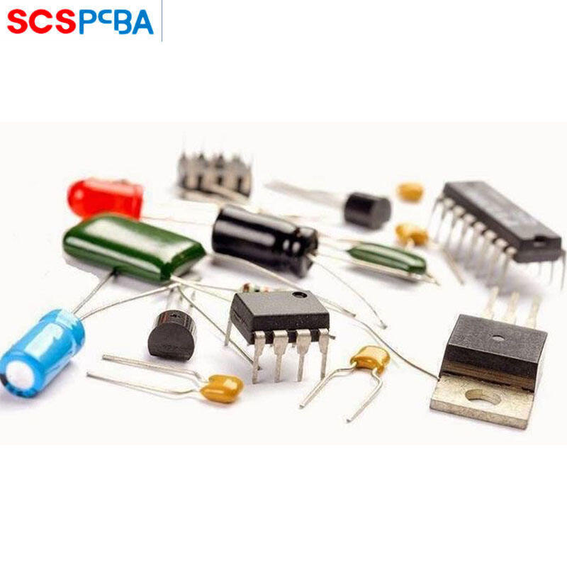
In order for the PCB to function as intend, components are assemble on it. Therefore, PCB functionality is of utmost importance. If a tiny SMT resistor have been misplace or a small track have been cut from the PcbPcba manufacturer, the PCB may not work. It is, therefore, necessary to assemble the components in a proper manner. PCBs are call PCBAs or Assembled PCBs when they are assemble with components.
Based on the specifications provided by clients or users, PCBs can be complex or simple. There are also different PCB sizes depending on the requirements.
We will discuss both the automated and manual assembly processes for PCBs.
The design and layering of PCBs
The signal layers between the outer layers are multiple, as we described above. Therefore, our next topic will be the types of outer layers and their functionality.
1- Substrate:
This rigid board make of FR-4 material is use for stuffing or soldering components. PCBs are make rigid by this.
2- Copper Layer:
Top and bottom copper traces are create by applying copper foil to both sides of the PCB.
3- Solder Mask:
PCBs are covered with this layer on top and bottom. It isolates copper traces from each other to prevent short circuits and creates non-conductive regions on PCBs. The solder mask also prevents soldering on unwanted parts and ensures that solder only goes on holes and pads intended for soldering. SMT components are attached to the PADs, while THT components are attached to the holes on the PCB.
4- Silkscreen:
White labeling we see on PCB fabrication for component designations, like R1, C1, or descriptions on PCBs or company logos, is made from silkscreen layers. This silkscreen layer provides PCB information.
Packaging and shipping
The final step in the production process is packaging and shipping your products based on your instructions. The process of processing PCBA electronic products is relatively complex. To control quality, meet customer requirements, and deliver the perfect product, each employee needs to work together and follow the production process strictly.
When it comes to achieving the features and functionalities you want from your PCB, PCB assembly is critical. All designed features, component innovations, and supply chain efficiencies come together during assembly. In addition, in order to maintain component integrity and test PCB quality according to your requirements, we have installed systems throughout the process.
Assemblies are placed, soldered, inserted, cleared, and inspected. Our assembly capabilities include Surface Mounting or Through-Hole Technology, as well as BOM Component Verification for quality control.
Pcb Assembly | Pcb Assembly Services | Pcba Manufacturing | Printed Circuit Board Assembly | Electronic Components | Electronic Manufacturing Services | Pcb Assembly Manufacturer | Prototype Pcb Assembly